
The semiconductor industry is projected to grow by 11.2% in 2025, reaching a massive US$700.9 billion market. This remarkable expansion is primarily fuelled by the adoption of artificial intelligence and the continued proliferation of smartphones. Understanding this complex supply chain highlights critical investment opportunities and bottlenecks that determine which companies achieve outsized returns. In this article, we will examine each stage of manufacturing, from raw silicon to finished chips, each offering a distinct investment thesis and risk profile.
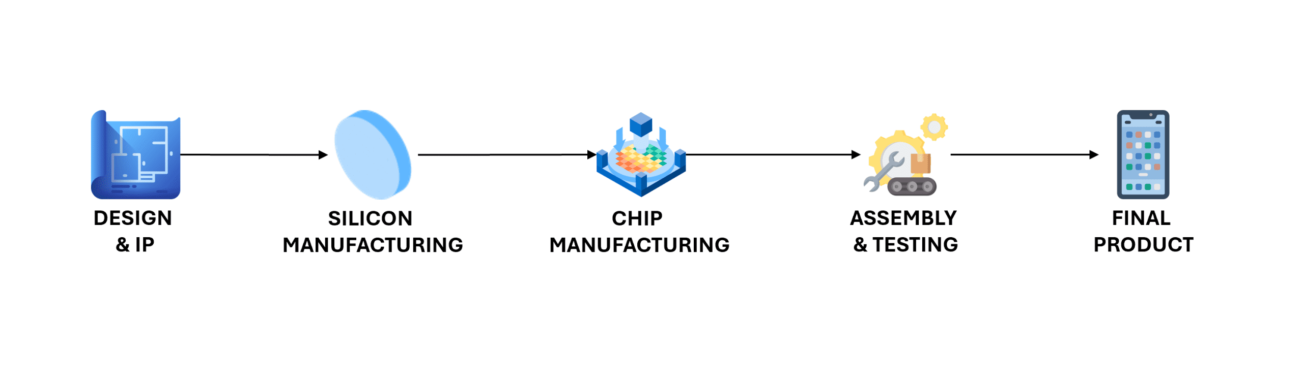
Stage 1: Design and IP development
Semiconductor design involves creating the fundamental architecture and circuit layouts that determine how billions of transistors work together. This stage operates on high-margin, asset-light business models where intellectual property generates recurring licensing revenue streams, and they do not manufacture the chip themselves.
At this stage, it is essential to highlight ARM Holdings, majority-owned by SoftBank (87%), which dominates mobile processor architectures through its licensing model. ARM provides the blueprints, essentially the common language and design standards, for chips that power 99% of smartphones worldwide. Once the architecture is set, engineers rely on Electronic Design Automation (EDA) software to design, test, and verify circuits and chips before manufacturing. The EDA market is led by Synopsys (31% market share) and Cadence (30% market share), whose critical design tools foster sticky customer relationships and generate highly predictable revenue streams.
Major semiconductor companies then leverage these foundational technologies through different business models. Companies like Apple, Qualcomm, and NVIDIA operate as “fabless” companies; they design chips but do not own any manufacturing facilities, instead outsourcing production to specialised foundries. This asset-light approach allows them to focus on innovation and design while avoiding the massive capital requirements of building fabs. For example, Apple designs custom A-series processors exclusively for its devices, Qualcomm creates Snapdragon platforms for multiple Android manufacturers, while NVIDIA develops GPU architectures that dominate AI computing.
Stage 2: Wafer production
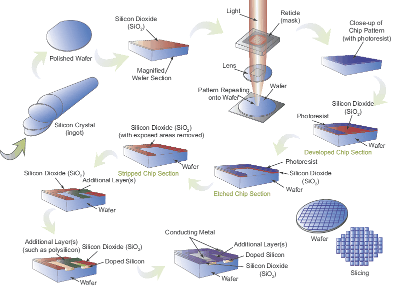
Once the design phase is complete, the actual manufacturing process begins with silicon wafer manufacturing. It starts with ordinary sand (silicon dioxide or silica), which is purified to create ultra-pure, cylindrical silicon ingots. These ingots are sliced into thin wafers (large, round disks) that serve as the foundation for chip production. The wafers must be atomically smooth, as even the slightest imperfection can compromise the billions of transistors built on top.
Japanese companies Shin-Etsu Chemical and SUMCO together control 57% of global wafer production as of 2020, with Shin-Etsu holding the lead at 32%. This stage of the supply chain demands enormous capital investment and decades of process expertise, creating naturally high barriers to entry and reinforcing the industry’s oligopolistic structure.
Stage 3: Fabrication equipment and manufacturing
Next, fabrication is the most sophisticated manufacturing process in any industry, where atomic-level precision meets industrial scale. Multiple complex processes transform blank wafers into functional semiconductors through processes like photolithography, etching, deposition, and ion implantation.
ASML maintains monopoly control over the Extreme Ultraviolet (EUV) lithography systems essential for producing advanced chips below 7 nanometres. Its top-of-the-line machines, like the high-numerical-aperture (high NA) EUV, can cost up to US$380 million, with an average lead time of around 12 to 18 months, giving ASML unprecedented pricing power. EUV technology uses light wavelengths so short they are absorbed by air and glass, requiring the entire system to operate in a vacuum. To date, no competitor has been able to replicate ASML’s decades of sustained investment and engineering expertise.
Other critical equipment suppliers play indispensable roles across different stages of chip fabrication. Applied Materials and Lam Research dominate etching processes that remove unwanted silicon, while Tokyo Electron provides tools across multiple fabrication steps. KLA Corporation specialises in inspection systems that detect defects with extreme precision. These companies not only benefit from equipment sales but also generate recurring revenue through consumables, long-term service contracts, and ongoing technology upgrades.
Leading foundries such as TSMC, Intel, and Samsung operate the advanced fabrication facilities that utilise this equipment. Foundries are specialized manufacturers that produce chips designed by fabless companies, effectively shouldering the immense cost of manufacturing infrastructure while their customers concentrate on design and marketing. TSMC dominates the market with a 67.6% share and commands premium pricing for its cutting-edge processes, making it the world’s largest contract chipmaker. Intel, by contrast, follows an Integrated Device Manufacturer (IDM) model, designing and producing its own chips, though it is now expanding into contract manufacturing through Intel Foundry Services (IFS) in an effort to compete directly with TSMC.
Stage 4: Assembly, testing and packaging
After fabrication, individual chips must be cut from the wafers, tested for functionality, and packaged for protection and electrical connectivity. The Automated Test Equipment (ATE) market is dominated by a duopoly: Advantest and Teradyne, which together control about 80% of the market. Advantest leads with roughly 50% share, compared to Teradyne’s 30%. Their equipment conducts comprehensive electrical testing to ensure each chip performs reliably under a wide range of operating conditions.
Outsourced Semiconductor Assembly and Test (OSAT) providers such as ASE and Amkor manage the assembly and packaging stages on behalf of fabless companies and foundries. Historically, OSATs operated as low-margin businesses centred on basic packaging. However, the rise of advanced packaging, driven by the demands of AI chips, is reshaping the industry. Modern processors increasingly integrate multiple chips into a single package using chiplet designs and 3D stacking, significantly boosting performance.
This shift toward advanced packaging is creating new growth opportunities for equipment suppliers and substrate manufacturers, as packaging evolves from a commoditized step into a sophisticated layer of technology integration. For the scope of this article, we will not explore these developments in depth.
Stage 5: Final product and market applications
The last stage is the final product. Apple exemplifies vertical integration by using its custom-designed A-series and M-series chips exclusively in iPhones and iPads, capturing maximum value through seamless hardware-software integration. NVIDIA, on the other hand, has emerged as the leading supplier of AI infrastructure. Its H100 and H200 chips power countless AI applications, and are sold primarily to hyperscale cloud providers such as Microsoft, Google, and Amazon.
Qualcomm supplies its Snapdragon processors to a wide range of Android manufacturers – including Samsung, Xiaomi, and OnePlus – creating diversified revenue streams through broad market penetration. At the same time, hyperscale companies such as Google, Amazon, and Microsoft are increasingly designing custom chips for their own cloud services. Google’s TPUs and Amazon’s Graviton processors exemplify this vertical integration trend, which has the potential to reshape traditional supplier relationships and reduce dependence on third-party chip providers.
The fifth perspective
After reviewing the semiconductor supply chain, it is clear that companies are highly specialized within distinct segments and geographically scattered across the globe. This concentration creates systemic risks: Taiwan hosts TSMC’s advanced facilities, South Korea dominates memory production through Samsung and SK Hynix, and the Netherlands is home to ASML’s irreplaceable EUV technology. Adding to this, the industry’s long manufacturing cycles and massive capital requirements, often exceeding US$15 billion per fabrication plant, further limit competition to a handful of entrenched players.
The surge in AI adoption has driven unprecedented demand for semiconductors, fuelling a multiyear growth cycle that disproportionately benefits companies with monopolistic positions and technological leadership. This article only scratches the surface; each stage of the supply chain is highly specialized and deeply technical. For investors, the opportunity lies in identifying a stage or company that aligns with your thesis—and digging deeper to capture the tailwinds of this transformative industry.